Future Intel CPUs could be cobbled together using different parts

 Image: Gordon Mah Ung
Today’s processors, made using a single continuous slab of silicon, may soon give way to multiple chips interconnected at high speeds, Intel said Tuesday morning.
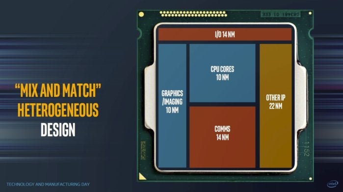
Intel said its new Embedded Multi-die Interconnect Bridge, or EMIB, technology would let a 22nm chip connect to a 10nm chip and a 14nm chip, all on the same processor.
“For example, we can mix high-performance blocks of silicon and IP together with low-power elements made from different nodes for extreme optimization,” said Intel’s Murthy Renduchintala, who heads the Client, IoT, and Systems Architecture Group.
That’s a radical departure from how the company has constructed most CPUs and SoCs, where all components of a CPU or SoC are built on the same process.
Renduchintala didn’t commit EMIB to any particular upcoming SoC or CPU but said it was clear the tech would play a large role in near-term and long-term products from Intel.
Renduchintala said EMIB can hit “multi hundreds of gigabytes” speeds while reducing latency by four times over traditional multichip techniques.
“It’s truly a transformational technology for Intel,” he said.
 Intel
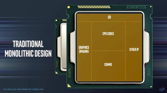
IntelToday’s CPUs are monolithic designs with all of the functionality built on the same process technology.
With EMIB, Intel could build the CPU and graphics cores on a bleeding-edge 10nm process and keep lower-performance components on 14nm. Still other parts that might actually benefit from being fabbed on, say, the 22nm process, such as power circuits, could stick to the larger process. At one point Intel dabbled with integrating the voltage regulation into the CPU with its 4th-gen Haswell and 5th-gen Broadwell chips. With 6th-gen Skylake and 7th-gen Kaby Lake though, the integrated voltage regulation was yanked, which some believed was due to problems scaling the fully integrated voltage regulator down to 14nm. An EMIB version could potentially keep the FIVR at 22nm.
 Intel
IntelFuture CPUs from Intel could fuse together multiple process technologies.
It isn’t the first time Intel has considered fusing two chips together in one CPU. The original Pentium Pro design was a multichip package as was the Core 2 Quad series of CPUs.
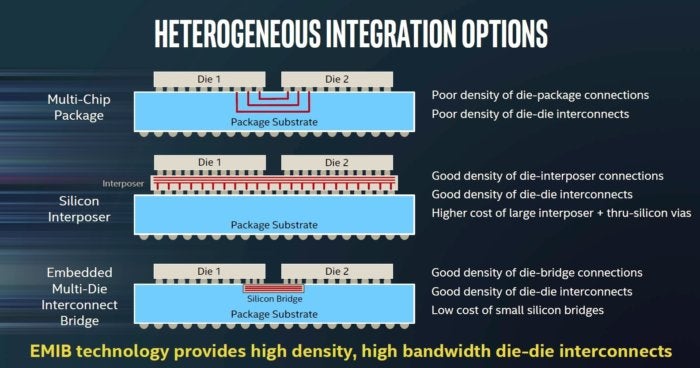
EMIB is far more advanced though, and is constructed within the silicon itself. A traditional multichip package design runs wires through the substrate that the chips are mounted to. That limits the amount of wires and speeds they can run at.
Another method is to use a silicon interposer to connect the dies. While this yields high wire density and high performance, it’s expensive to manufacturer.
EMIB essentially makes it far easier to combine chips without giving up much of the performance.
 Intel
IntelIntel says its Embedded Multi-die Interconnect Bridge is more cost effective than methods that use an interposer to connect chips and offers far better performance than multichip package designs.
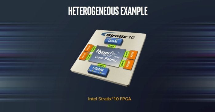
Although Intel made a point of highlighting EMIB at its technology and manufacturing day for press and financial analysts, this isn’t EMIB’s first use. Intel actually introduced it with the Altera Stratix 10, which used EMID to construct the SoC.
 Intel
IntelIntel is already fabbing the Altera Stratix 10 by joining together multiple chips using its new EMIB interconnect.


